Tuesday 24 April 2018

Transistor

Introduction

Transistor is a semiconductor device which  is used as an electronic switch and as a signal amplifier. It is a semiconductor device that revolutionized the electronic industry. It replaced vacuum diode that was used in most appliances before the invention of transistor. 


Vacuum tube and transistor
The disadvantages of vacuum diodes:
  • bulky (large in size)
  • High power consumption because works on thermionic emission
  • Glass tubes are fragile 
  • Higher operating voltage requirement
  • Shorter life span

Advantages of transistors
  • Usually lower cost and smaller than tubes, especially in small-signal circuits.
  • Lower power consumption, less waste heat
  • Can operate on lower-voltage supplies.
  • Long life span
There are two main classification of transistor. One is called Bipolar Junction Transistor (BJT) and the other, Field Effect Transistor (FET). In this post only BJT will be discussed.

Bipolar Junction Transistor

Structure and Symbol

There are two types of BJT, one is NPN and the other one PNP. It is made up of two PN junctions connected back to back. The structure of PNP and NPN looks like below.


The symbol of PNP and NPN and their matching structure.


Note that the arrow in the symbol indicates the direction of current flow.

The transistor can be visualized as two diodes connected back to back as shown below.


Some typical features of the PNP or NPN layers
  • Base layer is made very thin compared to emitter and collector
  • Emitter is heavily doped ( largest carrier quantity), Base is lightly doped ( lowest carrier quantity)  and collector has medium doping level.


Transistor applications
Two most fundamental application of transistor is a switch and as an amplifier.

Transistor as Switch

BJT is a current controlled device. The base current controls the Emitter to Collector current. When the base current is zero, the transistor is in the OFF mode. No current will flow in the Emitter to Collector path. When sufficient base current flows then the transistor will turn on and current will flow in the  Emitter to collector path.


Transistor as an Amplifier

Transistor can be configured to work as an amplifier, which is to enlarge or magnify the input signal level as shown below.


Low power and High Power transistor

Low power transistor are designed to work with small currents  while high power transistors are made to handle large amount of current. Power transistors should be able to handle the heat generated during its operation. Normally power transistors have heat sink to dissipate heat.

Low power transistors


Transistors does not produce heat during OFF mode because no current is flowing during this time.  During complete ON mode also the heat is not very high because the resistance inside the transistor is small, hence heat loss is small. However during partial ON, the resistance between emitter and collector is quite high and this can produce heat that should be dissipated or else the transistor will melt down.
High power transistors

High Power transistors

Transistor Operation Modes

Unlike resistors, which has a linear relationship between voltage and current, transistors are non-linear devices. They have three important  modes of operation.

Three transistor operation modes are:


  • Saturation – The transistor acts like a short circuit. Current freely flows from collector to emitter.
  • Cut-off – The transistor acts like an open circuit. No current flows from collector to emitter.
Saturation and cutoff modes are used in switching operation.
  • Active – The current from collector to emitter is proportional to the current flowing into the base.
The active mode is used when transistors are used for amplification


To determine which mode a transistor is in, we need to look at the voltages on each of the three pins E,C and B and how they relate to each other. The voltages from base to emitter (VBE), and  from the base to collector (VBC) set the transistor’s mode:

Saturation Mode

In the saturation mode, both the junctions of the transistor (emitter to base and collector to base) are forward biased. In other words, if we assume two p-n junctions as two p-n junction diodes, both the diodes are forward biased in saturation mode. We know that in forward bias condition, current flows through the device. Hence, electric current flows through the transistor.


Cutoff Mode

In the cutoff mode, both the junctions of the transistor (emitter to base and collector to base) are reverse biased. In other words, if we assume two p-n junctions as two p-n junction diodes, both the diodes are reverse biased in cutoff mode. We know that in reverse bias condition, no current flows through the device. Hence, no current flows through the transistor. Therefore, the transistor is in off state and acts like an open switch.


From the above discussion, we can say that by operating the transistor in saturation and cutoff region, we can use the transistor as an ON/OFF switch.

Active Mode

In the active mode, one junction (emitter to base) is forward biased and another junction (collector to base) is reverse biased. In other words, if we assume two p-n junctions as two p-n junction diodes, one diode will be forward biased and another diode will be reverse biased.


The active mode of operation is used for the amplification of current and it is a very common and useful mode.

Water analogy of Action Mode

In the action mode, the base current IB controls the amount of emitter to collector current. As shown  in diagram below, when IB is zero, the plunger closes the path from Collector to Emitter. When there is a small flow in base current, the plunger moves up and allow large current to flow in the emitter-collector path. When the base water/current is increased, a proportional increase occurs in the collector current.

Transistor current flow and current equation


IE = IC + IB

Transistor application examples

A. Switching circuits 
A small base current switches a larger collector current. Hence turning on a load.


LED B will glow dimly because only small current is flowing to the base. However LED C will be bright because higher current flow from collector to emitter.
The amplification amount is determined by dc current gain factor:

hFE = IC /IB


Example of hFE calculation
1. 


2.


B. Transistor amplification

One simple application where a transistor circuit can be used as an amplifier will be to increase the output from a microphone.


Darlington Pair 
Darlington pair is used to achieve very high gain! It comprises of two  bipolar transistors that are coupled in order to deliver a very high-current gain from a low-base current. The emitter of the input transistor is connected to the base terminal of the output transistor, base and collectors of these transistors are wired together. Therefore, the current that is amplified by the first transistor and then by the second transistor.


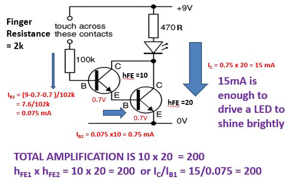
Touch sensor using Darlington pair


Rain sensor using Darlington Pair


Example of Darlington pair calculations


Transistor Configuration

A transistor can be connected in the following three different configurations.


To identify the configuration do the following steps:
  • Check to which terminal ( E,B or C) is the input connected 
  • Check to which terminal ( E,B or C) is the output connected 
  • The remaining terminal is the common one!
Try to check the type of configuration for the following.

a.

b. 

c. 
Answer : a. CC  b. CE  c. CB


Sunday 8 April 2018

Resistor and Capacitor in AC Circuit

Let us look at the behaviour of capacitor in ac circuit.Capacitor will create opposition to current flow which is called as reactance. The reactance depends of frequency and calculated using the formula:
\[\large Xc= \frac{1}{2\pi fC}\]
In pure capacitive circuit also the voltage lags the current by 90°


In a R-C circuit the opposition to current comes from both the resistor and also from the capacitor. The combined opposition is called impedance (Z).

Analysis of R-C circuit
R1 causes opposition to current  = 5Ω
C1 causes opposition to current =\[\large Xc= \frac{1}{2\pi 60\times 100\times 10^{-6}} = 26.5\]

\[\large Z=\sqrt{R^{2}+X^{2}}\]
\[\large Z=\sqrt{5^{2}+26.5^{2}} = 26.96\]


Current in the circuit = V /Z = 100 /26.96 = 3.71A
We can find other parameters such as voltage drop across components, true power and reactive power.

Voltage drop across R
VR = IR = 3.71 x 5 = 18.55V

Voltage drop across C
V =IX = 3.71 x 26.5 = 98.32V

Voltage supplied ( or Total voltage) =Vector addition of VR and VC

\[\large V_{T}=\sqrt{V_{R}^{2}+V_{C}^{2}}\]
\[\large V_{T}=\sqrt{18.55^{2}+98.32^{2}} = 100\]

Try to calculate the true power and reactive power.


Saturday 7 April 2018

Resistor and Inductor in AC circuit

Basic behaviour of passive components in AC

The three passive components in electricity are resistor, inductor and capacitor. All these components impede (resist) current flow in an ac circuit. Resistor imposes resistance while inductor  and capacitor impose  reactance. Both these quantities are measured  in ohms. Just think of reactance as resistance in inductor and capacitor. 
The current and voltage behaviour of these components are quite interesting. In a pure resistive circuit, the current and voltage are always in phase with each other. While in a pure  inductive circuit, the applied voltage is ahead of current by 90°. 


In pure resistive circuit
Image result for voltage and current relation in resistor in ac


In pure inductive circuit 

The applied voltage leads the current by 90°. The applied voltage comes from the AC power supply. 

There is also another type of voltage which produced inside inductor which is created whenever there is change in current and this is called  induced voltage. The induced voltage always opposes the applied( source) voltage. Thus it is  always 180° apart from the applied voltage.

Phasor diagram of V applied, Current I and V induced.


For understanding we can compare pure resistive and pure inductive in one phasor diagram like shown below,


What if we have an AC circuit that has both resistor and inductor in it? What will be the phase difference between the applied voltage and current in the circuit?
In a circuit that has both resistance and inductance, the source voltage and source current (total current) will differ by an angle between 0 and 90°. The angle depends on the ratio of the R and L value.

R-L Series in AC circuit

Lets analyze the circuit below and determine all the circuit parameters such as current, voltage drop across components and power.

Reactance by L1 :  XL = 2πf L = 2 x 3.142 x 50 x 0.01 = 3.142 Ω
Resistance by R1 = 5Ω
The total obstacles to current flow is called impedance ( Z) whereby Z is the vector addition of R and X.

Impedance diagram

Image result for impedance of R and L vector addition

In vector addition we cannot simply add the values directly unless there both quantities are in the same direction. In the R-L case we cannot just add the value of R and X even if they are in series.

\[\large Z= \sqrt{R^{2}+X^{2}}\]

Applying the formula in the analysis:


\[\large Z= \sqrt{5^{2}+3.142^{2}} = 5.90\]

I = V/Z
= 100/5.9 = 16.95A

Voltage drop across resistor
V = IR = 16.95 x 5 = 84.75V

Voltage drop across inductor
VL = IX = 16.95 x 3.142 = 53.26 V


When both voltages are added directly, the total becomes 84.75 + 53.26 = 138.0 V , which exceeds our supply voltage of 100V.
This is not possible. 

Again, remember that these quantities are not in the same phase. Vector addition must be done to find the total voltage or the supplied voltage and not normal addition. 

\[\large V_{T}= \sqrt{V_{R}^{2}+V_{X}^{2}}\]


\[\large V_{T}= \sqrt{84.75^{2}+ 53.26^{2}} = 100\]


Leading and Lagging self-test

From the waveform below, can you identify which waveform is in phase, which is leading and lagging??


Tuesday 3 April 2018

Diodes

Introduction to Diode

Diode is like a one way electronic switch. One way means that current can only flow in one direction.
Electronics switch means that no manual on/off operation required but can be controlled by suitable voltage application.
The base material to make diode is semiconductor  such as Germanium and Silicon. These semiconductor materials in their pure stage are not very conductive. (That is why they are called semiconductor). To increase their electricity carrier property, they are doped (infused) with some other elements such as aluminum( group III in periodic table)  and phosphorus ( group 5 in periodic table). A silicon/germanium doped with aluminum will produce a P type ( more positive carriers) while silicon / germanium doped with phosphorus will produce N type ( more negative carriers).
The diode is made by combining P and N type material together. The P type is called anode and the N type is called cathode (K).


As mentioned earlier, diode behaves like a switch that conduct current in one direction only. Which direction is the flow of current? Well follow the sign of the diode, the triangle looks like the arrow head! Current flows in that direction. If diode behaves like a electronic switch, then you can turn it ON or OFF electronically but how ??
To turn on a diode, the anode ( P side) must be more positive than the cathode side by at least 0.6/0.7V for silicon and 0.3V for Germanium. This is called the threshold voltage. It is the minimum voltage required to turn on a diode. 
However for LED type of diodes, the voltage can be about 1.5V depending on the color of the LED. This voltage requirements are for practical diodes (used in real life). For ideal diodes, as long as anode is more positive than cathode, the diode conducts current. Hence the threshold voltage for ideal diode is 0V. In reality ideal diodes do not exist. There is always a minimum threshold voltage required to turn on a diode.

Different types of diodes based on application

a. Light Emitting Diodes  (LED)


Different colored led requires different threshold voltage to turn on. In diagram below, the green led requires 2.1V while the red led needs only 1.7V. 


b. Rectifier diode


A rectifier diode lets electrical current flow in only one direction and is mainly used for power supply operation. Rectifier diodes can handle higher current flow than regular diodes and are generally used in order to change alternating current into direct current.


c. zener diode

Zener diode is quite special and different  from other types of diode. In forward bias, it works as normal diode. In reverse bias, when reverse voltage across  Zener diode is increase to rated value, the voltage drop across diode becomes steady ( fixed and will not increase any more). This voltage drop is known as zener voltage and this property is used to regulate voltage across load. The load will not get damaged by


Self-Test

Check your understanding by answering the following questionnaires.
https://docs.google.com/forms/d/e/1FAIpQLSeAiqbW72y09nwxCj7725K5HeEjkHvck6SE1GsdY0sgiKG8pg/viewform?usp=sf_link

Diode operation, testing and application

A. Diode operation

1. Forward Bias Mode ( FB )

For diode to be in a forward bias mode (conduction mode), the anode must be connected towards the positive side of the voltage source and the cathode towards the negative side of the source. In this mode, the diode behaves similar to a closed switch. The resistance inside diode is very low (a few ohms).  
There can be other components between the diode and voltage source such as resistors but it can be still be in FB mode as long the anode is directed towards the positive side of voltage source.
In the following diagram, the lamp has a resistance of 5Ω and diode threshold voltage is 0.7V.


The voltmeter shows a drop of  about 0.7V across the diode and 4.3V across the lamp. Use Ohm's law to calculate the current value in the circuit.

2. Reverse Bias mode (RB)

When the anode is connected towards the negative of the power supply and the cathode towards the positive side, then the diode will be in the reverse bias mode (cut-off mode). Current cannot pass through the diode because of the high resistance value (in megaohm range) inside the diode. It is similar to a switch that is in an open state. Due to the high resistance of diode, almost all of the voltage from the supply will fall/drop across the diode and none across the load/lamp. The current value is almost zero.

The meter reading shows almost 5V across the diode and 0.00002V across lamp. Don't forget the multiplier x10^-3 on the right multimeter.


B. Diode Testing

How to test diodes - there are two ways:

a. Use diode test mode which provides voltage reading
b. Use resistance measurement mode

1. Diode test mode

Digital multimeters can test diodes using the diode test mode. A good diode gives a reading between 0.5V to 0.8V in the forward bias mode for silicon diode. A good Germanium diode gives reading between 0.2V to 0.3V. 
In reverse bias, both silicon and germanium will show OL ( open load).


2. Resistance measurement

Analog meters such as ohmmeter does not have a diode test mode. In this case, we can use resistance measurement to check if the diode is in good condition or not. A good diode shows a reading of less than 100 ohm in forward bias whereas in reverse bias mode it shows more than 1000 MΩ.


C. Diode applications

1. Rectification - conversion of AC signal to DC signal

1.1 Half wave rectifier

Constructed using a single diode and a load.


The waveform before the diode and after the diode were plotted using an oscilloscope. It can be seen that the negative cycle of the input wave has been cut off by the diode because during this part of the cycle, the diode is in the reverse bias mode or in the off state. No conduction of current takes place during this time. Also notice that the the final peak voltage is always about 0.6 -0.8V less than the input peak voltage. Why is that? ( Still remember the threshold voltage that diode requires for it to enter the conduction mode!)


The output from a half wave rectifier is a DC but even though current flows in one direction it still not a steady DC. The DC value fluctuates in the positive direction. Hence it is still not suitable to be used to drive most loads.The average output voltage of the rectified wave can be calculated using the formula:


Vave =  Vp/π      Vp =Peak output voltage

Example:
Answer the following questions based on figure below.


a. Is the transformer a step up or step down type?
b. State the peak voltage value at the primary and secondary side.
c. Type of signal ( AC/DC) at point A, B and C
d. The difference in peak value between point B and C.
e. The average value at output.
f. Plot the graph of the waveform at point B and C.

Answers
a. Step-down
b. 240V , 12V
c. AC, AC, DC ( fluctuating DC)
d. About 0.7V
e. 3.72 V


Half wave rectifier with smoother circuit


As we have seen previously that the fluctuating DC is still not suitable for driving loads. Hence we have to somehow make it a steady DC voltage. This can be done by fixing a capacitor parallel to the load. Capacitors stores charge or electricity. When the input voltage reaches the peak, the capacitor will be also be fully charged and keeps this charge. As the input voltage decreases from the peak value and become less than the capacitor, it is time for capacitor to release its charge into the load. Capacitor acts as a backup to provide energy to the load.

The diagrams below show the output for different values of capacitors. 
                       C = 10uF

                     C=100uF


                   C = 300uF


                             C = 1000uF

The figure below shows the area/region of the waveform where the capacitor gets charged up and where it discharges itself.


What is Ripple voltage?

The fluctuation of the dc value from the maximum to its minimum is called ripple as shown in diagram below.
Capacitor is used to remove the ripples!!

1.2 Full Wave Rectifier

A Full Wave Rectifier is a circuit, which converts an ac voltage into a pulsating dc voltage using both half cycles of the applied ac voltage. It uses 4 rectifier diodes forming a shape to looks like a bridge, hence the name bridge rectifier. A real life bridge rectifier looks like picture below. 

It is connected to an AC supply and  load as figure below.


Operation of full wave rectifier ( without smoothing)

Positive half cycle


Negative half cycle


Full wave rectifier output waveform
Average output voltage of  full wave rectifier ( before smoothing effect) is given by the formula below.

Vave = 2Vp/π


Comparison between full wave and half wave rectification waveforms


Removing ripple in full wave bridge rectifier

Again, capacitors are used to remove ripple


2. Voltage Regulation using Diode and Zener Diode

The function of a regulator is to provide a constant output voltage to a load connected in parallel with it in spite of the ripples in the supply voltage. The best way will be by using zener diode. However diodes can also be used. Let's see how diode works as voltage regulators.

Using diode to regulate voltage across load

Three silicon rectifier diodes in series are placed parallel to the load. Each diode needs 0.7V to turn on. In total 2.1V is all the is needed for current to flow through this path. The voltage across the load will also be fixed to this potential difference. Even if the rectifier output increases, the voltage across the load maintains at 2.1V.
How many rectifier diodes are needed if the load voltage is to be regulated to 7V?

Using Zener diode to regulate voltage

Lets look at symbol and behaviour of zener diode. Zener diode are specially made diodes which are intended to work in the reverse bias mode and not in the forward bias mode. Hence when we connect a zener parallel to the load, the cathode must always be connected to the positive side of the voltage source.


Zener diode comes in different Vz values. We need to use one that suits the circuit intended
An example using Multisim Live circuit simulator is shown below.


https://www.multisim.com/
Multisim Live is a free, online circuit simulator that includes SPICE software, which lets you create, learn and share circuits and electronics online.